# Groundbreaking Achievement in Graphene Semiconductor Development
Written on
Chapter 1: The Rise of Graphene
The discovery of graphene has emerged as a pivotal moment in scientific innovation. Often referred to as a two-dimensional marvel, graphene is formed from a single layer of carbon atoms arranged in a hexagonal pattern. Its remarkable electronic properties, characterized by outstanding conductivity and mechanical durability, have positioned it as a leading candidate for next-generation semiconductors.
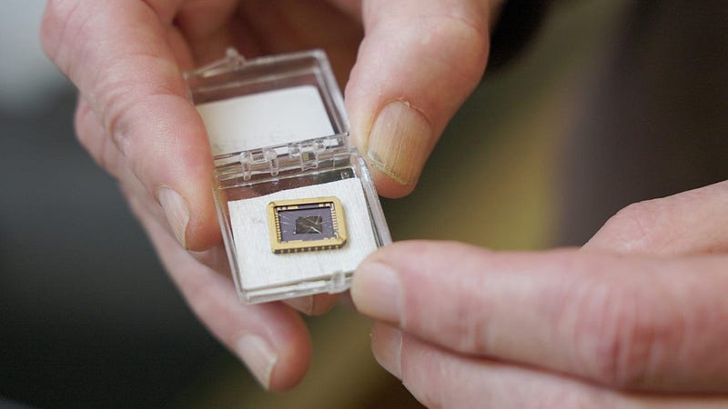
In an extraordinary breakthrough, scientists have successfully engineered the first functional semiconductor made from graphene. This achievement marks a significant departure from traditional silicon-based technologies, signaling a revolutionary shift in semiconductor design. It propels us toward a future where the limitless potential of graphene can overcome the constraints of conventional materials.
As silicon—the cornerstone of nearly all modern electronics—faces challenges posed by ever-increasing computing speeds and the demand for miniaturization, this development comes at an opportune moment. Walter de Heer, along with a team from Georgia Tech and Tianjin University in China, focused on creating a graphene semiconductor that integrates seamlessly with existing microelectronic processing techniques, an essential requirement for a viable alternative to silicon.

“We now have an extremely robust graphene semiconductor with 10 times the mobility of silicon, and which also has unique properties not available in silicon. But the story of our work for the past 10 years has been, ‘Can we get this material to be good enough to work?’”
~ Walter de Heer, Lead Researcher
Chapter 2: Overcoming Challenges in Graphene Research
Early in his career, De Heer began exploring carbon-based materials as potential semiconductors, eventually shifting his focus to 2D graphene in 2001. In this pioneering research, the team tackled a long-standing issue that has hindered graphene's progress for decades: the absence of a "band gap." This critical electronic property is essential for semiconductors to switch between on and off states. Historically, graphene did not possess a band gap, but recent advancements have transformed this narrative.
The research team developed a method to grow graphene on silicon carbide wafers using specialized furnaces, leading to the creation of epitaxial graphene—a single layer that forms on the crystal face of silicon carbide. Through careful refinement, they discovered that properly synthesized epitaxial graphene forms a chemical bond with silicon carbide, exhibiting semiconducting properties. The pursuit of material perfection has continued over the past decade through collaborative efforts between the two institutions.

Naturally, graphene exists as a semimetal, lacking the distinctive features of either a true semiconductor or metal. The primary function of a semiconductor is its ability to switch between on and off states under an electric field, a fundamental operation for transistors and traditional silicon-based electronics. A central challenge in graphene electronics research has been to find a way to effectively toggle the material, similar to silicon.
To create a functional transistor, significant manipulation of the semiconducting material is required, which poses risks of damaging its inherent properties. To assess the viability of their graphene platform, the team faced the challenge of measuring its electronic characteristics without causing harm. They employed a technique known as doping, which involves introducing atoms that "donate" electrons to the graphene. This method successfully measured the material’s conductivity without compromising its integrity.
Chapter 3: The Future of Electronics with Graphene
The measurements obtained by the team demonstrated that their graphene semiconductor possesses an impressive tenfold increase in mobility compared to silicon. This means that electrons can move through the material with minimal resistance, a property that directly correlates with improved computing speeds in electronic devices. Notably, their product stands as the only two-dimensional semiconductor currently exhibiting all essential characteristics for use in nanoelectronics.
Furthermore, its electrical properties surpass those of any other 2D semiconductors under development. Epitaxial graphene holds the potential to catalyze a paradigm shift in electronics, paving the way for entirely new technologies that leverage its unique attributes. This material enables the exploration of quantum mechanical wave properties of electrons, a crucial advancement for the field of quantum computing. Are we witnessing a Wright brothers’ moment in the evolution of electronics?
The complete research findings were published in the Journal of Nature.
Stay informed with the content that matters—Join my Mailing List.